1. 引言
钼酸铅(PbMoO4)是一种广泛应用的材料,在光催化、太阳能电池、污染物降解和农业等不同领域都有应用,同位素100Mo的存在也使得钼酸铅可以被用作双β衰变的检测器 [1] - [7] 。然而,这些应用都取决于钼酸铅的纯度。钼酸铅中的缺陷对材料的特性有很大影响。例如,由钼酸铅中的色心引起的光致变色效应对其在光学仪器中的应用是有限制的。值得一提的是,钼酸铅的晶体特性也受到晶体生长方法的强烈影响。掺杂剂、主要成分的偏差和紫外线辐射都会对钼酸铅的缺陷产生影响。因此,对钼酸铅中缺陷的研究对于控制晶体生长条件和避免其中的负面影响是必要的 [5] [8] - [14] 。
MoO3和PbO是PbMoO4生长的原始材料。MoO3和PbO具有不同的气压,PbO具有较高的挥发性 [15] 。因此,如果钼酸铅生在富氧的环境中,会形成大量的氧填隙。经过过去十年对钼酸铅材料的广泛研究,材料中空位缺陷对材料光学性质的影响已相对成熟。氧填隙缺陷是钼酸铅中典型的内在点缺陷,直接或间接地控制着材料的许多特性。然而,钼酸铅中氧填隙缺陷的研究结果仍然是目前研究中的一个空白,特别是对带电缺陷的缺陷形成能计算和缺陷的吸收谱与发射谱的计算 [16] [17] [18] [19] 。
M. Buryi等人利用EPR和TSL实验研究了钼酸铅单晶中的电荷捕获和能量转移过程 [20] 。实验结果对钼酸铅晶体中的电子跃迁有着很好的指导意义。在这项工作中,我们使用密度泛函理论(DFT) [7] [21] 计算了氧填隙的电子结构。我们采用Freysoldt-Neugebauer-Van de Walle (FNV) [22] 校正来抵消缺陷状态的周期性图像,以获得准确的缺陷形成能量。带隙是通过杂化泛函方法调整的。通过考虑电声耦合效应,研究了氧填隙的光学性质。
2. 计算方法
2.1. 计算模型
钼酸铅晶体(PMO)的原胞由12个原子组成,空间群结构为I41/a。在本次计算中我们使用的计算模型为钼酸铅原胞2 × 2 × 2扩胞之后得到的96个原子的晶胞 [23] 。我们通过在合适的位置加入一个氧原子在计算氧填隙的性质(如图1所示),氧填隙缺陷可能失去0个电子(OI),1个电子(
)或者2个电子(
)。
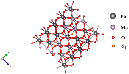
Figure 1. Lead molybdate with interstitial oxygen
图1. 含有氧填隙缺陷的钼酸铅晶胞
2.2. 计算参数设置
所有缺陷结构的结构优化使用Vienna Ab-initio Simulation Package (VASP) [24] 完成。电子之间的相互作用选择projector argument wave (PAW) [25] 方法进行描述,交换–相关势由generalized gradient approximation of Perdew-Becke-Ernzerh (GGA-PBE) [26] 方法描述。选用的价电子为:Mo:4d55s1,Pb:6s26p2,O:2s22p4。在计算中选择了800 eV的截断能和3 × 3 × 3的K点设置。
2.3. 带边修正
使用DFT计算的材料带隙值往往比真实值偏小,考虑到后续计算中电子跃迁的问题需要,必须要对此问题进行修正。我们使用杂化泛函(HSE06) [27] 来修正带隙问题,此时交换–相关函数为:
(1)
该方程描述了新的电子的交换–相关作用,可以通过调节参数
来获得更准确的带隙值。参数
对应Fock交换相关势和PBE交换相关势的权重。经过反复测试,我们在此次计算中设定
,计算得到的钼酸铅带隙值与实验值较为吻合。计算的对比结果我们列在表1中。
Table 1. Comparison of PMO bandgap values calculated using different functional functions with experimental values (in eV)
表1. 使用不同泛函计算的PMO带隙值与实验值的比较(单位:eV)
计算得到HSE与PBE的价带顶(VBM)与导带底(CBM)位置之后,我们进行带边修正,缺陷转化能级位置如图2所示。其中common reference level为公共参考能级。
3. 结果和讨论
3.1. 结构优化
在对含有氧填隙的晶体进行结构优化之后,氧填隙结构发生了明显的结构弛豫。在引入一个氧原子之后,填隙周围最近邻的原子离填隙的距离会发生变化,这是因为填隙周围的氧原子受到库仑力和机械力的作用。与完美晶体的结构相比,氧填隙一般呈现二价负电性(
),因此一旦产生填隙,由填隙引起的两类势将出现,其一是氧填隙引起的电动势,这将吸引填隙周围Pb2+和Mo6+,而将带负电的O2−推开:其二是由于填隙本身产生的机械势,填隙结构带带电后,将于周围的Mo6+成键,此时填隙与Mo6+之间的相互作用大于产生负电产生的电势,使得周围的Mo6+和O2−离子更加接近填隙位置,且此时填隙本身的机械势大于电势,推开了Pb2+。晶格弛豫情况在表2中给出。
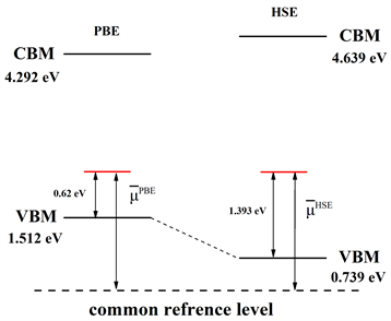
Figure 2. Schematic diagram of band edge correction for interstitial oxygen
图2. 氧填隙的带边修正示意图
Table 2. The distance variation between the vacancy and the nearest oxygen atom before and after structural relaxation (in Å)
表2. 结构优化前后填隙周围最近邻原子到氧填隙的位置(单位:Å)
3.2. 缺陷形成能修正
带电缺陷形成能的计算精度一直是业界难题,当一个晶胞中存在一个带电点缺陷之后,由于晶体的周期性排列,则带电缺陷也会周期性排列,带电缺陷之间就会产生不能忽略的相互作用,因此必须对缺陷形成能进行修正。
带电点缺陷的缺陷形成能可以表示为 [28] :
(2)
其中
表示含有缺陷晶体的总能量,
是完整晶体的总能量,
是氧的化学势,
指的是完美晶体的价带顶,
是费米能级位置,
为完整晶体和含有缺陷晶体的电势差。
即缺陷形成能的修正项,可以表示为:
(3)
其中
是晶格屏蔽能,
表示的短程势:
(4)
其中
为缺陷位置的电荷分布,n为背景电荷,加入背景电荷之后即可消除由于带电缺陷引起的静电相互作用,
为周期性结构中的长程电势分布,
为孤立点缺陷的长程电势分布,下面我们对方程(4)进行详细解释:
在缺陷附近,模型电荷与实际电势分布差异较大,在远离缺陷位置,两者电势分布非常接近,所以对于缺陷附近,我们选择加入短程电势。因此,首先应该确定缺陷位置的电荷分布:
(5)
进一步考虑带电缺陷周围电荷的电势,我们引入:
(6)
其中
带电量为q的缺陷电势分布,
为带电量为0的缺陷电势分布,二者相减本质即为电荷q产生的电势,又考虑到周期性结构与补偿电荷的存在,通过对实空间中的电势分布进行傅里叶变换,可以得到倒格子空间中的电势分布:
(7)
(8)
式(7)为考虑到周期性结构的电势分布。
计算孤立点缺陷形成能,周期性的带电缺陷之间有不真实的库仑相互作用,使用下式对该相互作用进行消除:
(9)
为了使计算收敛,计算对带电体系设置了了等量异号均匀分布的背景电荷。背景电荷实际体系并不存在,需要剔除它的影响:
(10)
其中
(11)
(12)
考虑了周期性结构之后,短程势应该为超原胞中所有点缺陷附近电势的叠加
(13)
其中
为倒格子基矢,则其他原胞的短程势即可忽略不计,因此,式(4.12)
(14)
其中,
,C以及介电常数
都可以通过DFT计算得到,
,至此,可以计算缺陷形成能的修正项。
缺陷电荷模型:
(15)
其中
为缺陷的中心位置,等式右边第一项是指数函数,第二项为高斯函数,高斯衰减速度大于指数衰减速度,因此,当电荷比较局域,
我们使用高斯衰减,x为选择函数的权重。
,
,是归一化常数。图3为氧填隙缺陷形成能修正短程势与长程势的拟合,图中虚线即是短程势,横坐标中间位置表示远离缺陷的位置,远离缺陷位置趋近于0,表示修正达到了良好的效果。
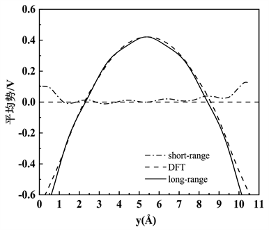
Figure 3. Correction of defect formation energy
图3. 缺陷形成能修正
我们在表3中给出修正前后的缺陷形成能。
Table 3. Interstitial oxygen defect formation energy with and without correction (in eV)
表3. 氧填隙缺陷修正前后的缺陷形成能(单位:eV)
3.3. 氧填隙的光学性质
在获得缺陷形成能和缺陷转化能级的位置之后,通过考虑电子–声子耦合效应,我们可以近似的计算出氧填隙缺陷对应的吸收光谱和发射光谱。
根据弗兰克–康登原理(Frank-Condon Principe) [29] ,我们使用公式(4)来计算发射谱 [30]
(16)
其中S表示黄昆因子,
(
为有效频率),
为高斯函数,
为零声子线。
平均声子能量。另外,用于计算有效质量的参数
,
,
代表原子,
,
为位移矢量。计算光谱的有效参数列于表4。
Table 4. Calculation of the effective parameters of the interstitial oxygen defect spectra
表4. 计算氧填隙缺陷光谱的有效参数
对于吸收谱的计算:
(17)
(18)
(19)
其中
是转化能量,
是声子能量;
是光子能量;
是贝塞尔函数。
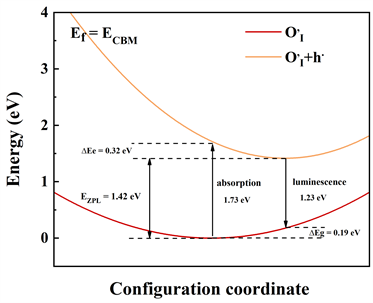
计算光谱的本质即考虑电子跃迁的问题。弗兰克–康登近似的优点在于能够大大减小计算量,得到可靠的计算结果。电子跃迁的结果可以使用位型坐标图来表示,它们代表了缺陷能级和价带顶之间的电子跃迁结果,氧填隙的光吸收和发射的一维位型坐标图(Configuration coordinate)如图4所示。
从图4中不难看出,
,
。费米能级的位置设置在价带顶时,在图3(a)中,缺陷能级获得价带之间发生空穴跃迁(
),图3(b)中,类似的过程同样发生在缺陷能级与价带之间发生空穴跃迁(
)。
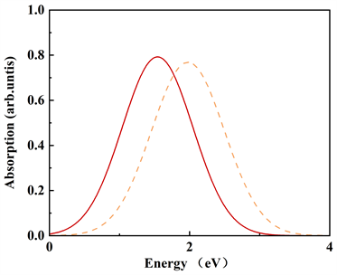
计算得到位型坐标之后,可以定量计算氧填隙归一化的吸收谱和发射谱。钼酸铅晶体的吸收和发射光谱展示在图5中,当费米能级设置在导带底时,可以看出氧填隙
和
的吸收峰位置在1.73 eV (717.5 nm)和2.15 eV (576 nm),发射峰的位置则在1.23 eV (1008.5 nm)和1.97 eV (629.4 nm)。其中576 nm的吸收峰非常接近580 nm [20] 的实验值。这样的结果表明,580 nm的实验吸收峰由很大的可能性来自于二价填隙氧
。另外的结果表明,一价氧填隙的吸收和发射波长应该处在红外区。
 (a)
(a) 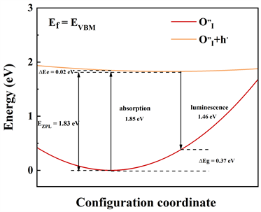 (b)
(b)
Figure 4. Configuration coordinate of
and
图4. 氧填隙
和
的位型坐标图
我们的计算结果中,缺陷形成能量已经得到很好修正,同时使用HSE方法计算得到与实验相一致的带隙值,在计算光谱的过程中,考虑了电声子耦合作用,得到与实验值相一致的结果。因此,我们预测,钼酸铅晶体中580 nm的吸收峰来自于氧填隙缺陷。我们计算的吸收和发射光谱描述了氧填隙缺陷空穴的抓捕和释放的过程,可以作为模型来期望更深入的了解白钨矿材料中的电荷捕获和电子跃迁的过程。
 (a)
(a) 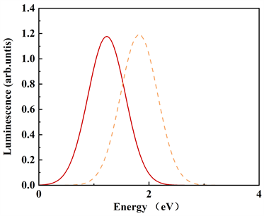 (b)
(b)
Figure 5. The absorption and luminescence spectra of
and
图5. 氧填隙
和
的发射谱和吸收谱
4. 结论
采用DFT方法,结合FNV修正方法计算得到了准确的缺陷形成能,使用杂化泛函HSE对带边进行了修正。计算了氧填隙的吸收峰在1.73 eV (717.5 nm)和2.15 eV (576 nm),发射峰的位置在1.23 eV (1008.5 nm)和1.97 eV (629.4 nm),我们预测580 nm的吸收带来自于二价氧填隙。考虑到氧的填隙缺陷会大量存在于钼酸铅晶体中,所以氧填隙是钼酸铅晶体中绿色吸收光的主要来源,我们期待进一步深化对这类材料光学性能的理论研究,为实际应用提供更多的指导。
致谢
感谢刘廷禹教授在文章撰写过程中的指导。感谢小组成员在文章调查过程中的帮助。
基金项目
本研究没有任何公共、商业或非盈利资助机构的任何具体资助。